Session 2 – Combinational Logic
In this second session, we turn our attention to the foundations of combinational logic. Our aim is to move from truth tables and Boolean expressions to a small set of concrete building blocks that we will reuse throughout the rest of the course.
By the end of this session, you should be able to:
- read and simplify small Boolean functions using Karnaugh maps,
- connect TTL‑style “chips” to their Verilog
moduleequivalents, and - recognise and use the standard combinational blocks: MUX/DEMUX, decoders/encoders, priority encoders, and comparators.
Boolean algebra refresher
We begin with Boolean algebra, the basic language in which combinational circuits are expressed. Every signal in our system is modeled as a Boolean variable—conventionally denoted A, B, C, and so on—taking one of two values: 0 for false or low, and 1 for true or high. On these variables, we define three primary operations. Logical conjunction, written A·B or A & B, yields 1 precisely when both A and B are 1. Logical disjunction, written A + B or A | B, yields 1 when at least one of A or B is 1. Logical negation, written A' or ~A, inverts the value of A. When needed, we also use exclusive-or, A ⊕ B or A ^ B, which yields 1 when its arguments differ.
These operators obey a small collection of algebraic laws that we use constantly to simplify expressions: identity (A + 0 = A, A·1 = A), domination (A + 1 = 1, A·0 = 0), idempotence (A + A = A, A·A = A), and complementation (A + A' = 1, A·A' = 0). Distribution allows us to factor and expand (A·(B + C) = A·B + A·C), and DeMorgan’s laws, (A·B)' = A' + B' and (A + B)' = A'·B', give us standard ways to move negation inward.
Given a Boolean function of several variables, we may always represent it by a truth table that enumerates every combination of inputs and the corresponding output. Each row in which the output is 1 corresponds to a minterm: an AND of all variables, each either complemented or uncomplemented so as to match that particular input pattern exactly. The OR of all such minterms is a sum‑of‑products expression that implements the function. This representation is canonical, but not usually minimal. To make hardware efficient, we therefore seek simpler, equivalent expressions.
Karnaugh maps (K‑maps)
Karnaugh maps provide a graphical aid for this simplification, particularly effective for functions of two, three, or four variables. A Karnaugh map rearranges the rows of the truth table into a grid whose row and column labels follow Gray code, ensuring that adjacent cells differ in only one input bit. We then place a 1 in each cell where the function is 1.
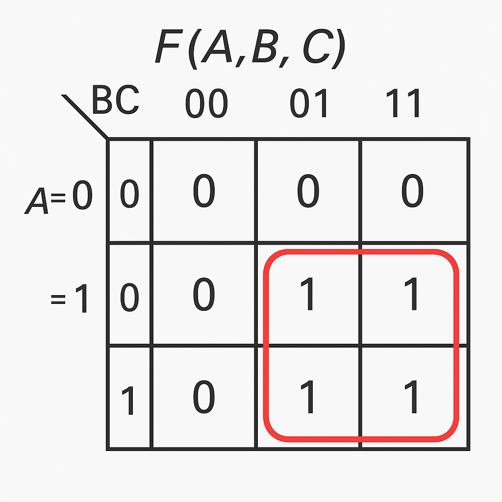
A 3‑variable K‑map picture
For F(A,B,C) with A on the rows and BC (in Gray code order) on the columns:
        BC
       00  01  11  10
     +----------------
A=0 |  0   0   1   0
A=1 |  0   1   1   1
In this example, the 1s correspond to the majority‑of‑three function (output is 1 when at least two inputs are 1). Adjacent 1s in this grid are what we group to obtain a simplified expression. You can also render this as an image in the site:
The simplification procedure consists of grouping adjacent ones into rectangular blocks whose areas are powers of two—1, 2, 4, 8, and so on—allowing the blocks to wrap around the edges of the map.
For each block, we identify the variables that remain constant throughout the block; these form a product term. Variables that change within the block disappear from the term. The final expression is the OR of one product term per block. The goal is to cover all ones with the fewest, largest possible blocks. When some input combinations are impossible or their outputs are irrelevant, we mark them as “don’t‑care” conditions. In the map, these can be treated as either 0 or 1 to enlarge groups and further simplify the resulting expression. A classic example is again the three‑input majority function, which, when simplified via a Karnaugh map, yields the elegant form F = A·B + A·C + B·C.
TTL chips to Verilog modules (mental picture)
Historically, digital designers worked with families of integrated circuits such as TTL, typified by the 74LS series:
- 74LS00 – 4 × 2‑input NAND gates
- 74LS138 – 3‑to‑8 decoder
- 74LS151 – 8‑to‑1 multiplexer
Each device is a fixed Boolean function in a package; a board diagram is just many such boxes wired together. In Verilog, each of these boxes corresponds to a module with inputs, outputs, and some combinational logic inside:
Structural designs instantiate these small modules and connect wires; behavioural descriptions write the Boolean expressions directly and let synthesis recreate the gates. In both views, you are manipulating the same combinational functions.
With that perspective in place, we can now introduce a compact set of canonical combinational modules that will recur throughout subsequent designs.
Canonical combinational blocks
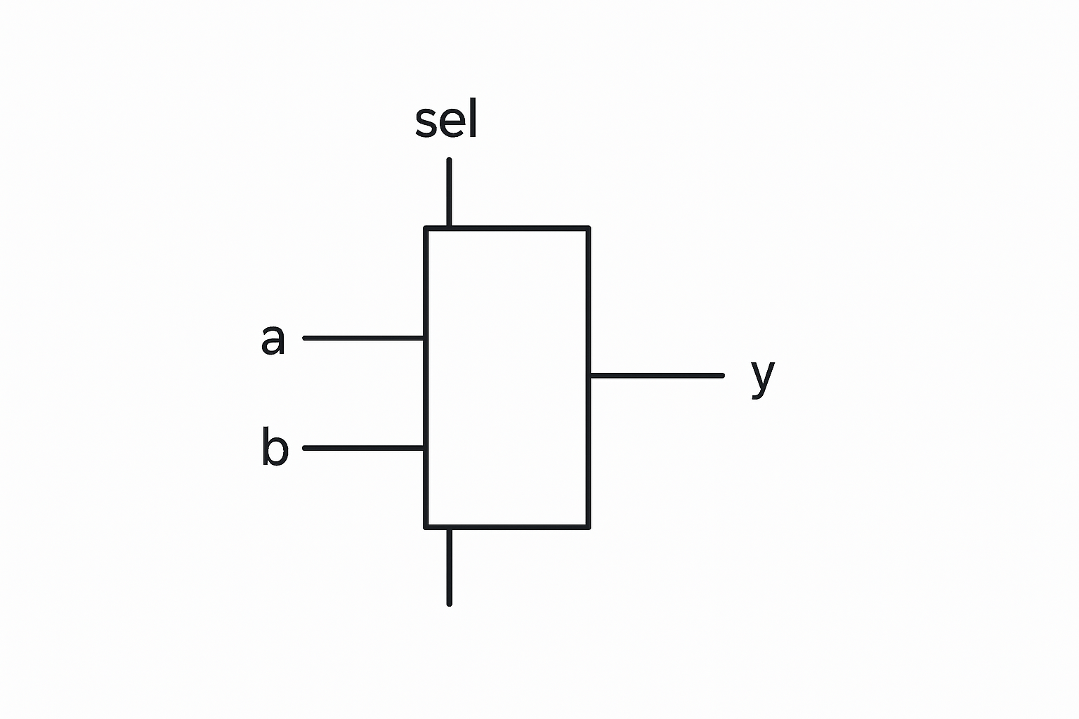
Multiplexer (MUX)
The multiplexer, or MUX, selects one of several data inputs and forwards it to a single output, under the control of select signals. Visually:
The simplest useful form is the 2‑to‑1 multiplexer, which chooses between two inputs a and b based on a one‑bit select sel. Its behavior can be captured in Verilog as follows:
module mux2 (
    input  wire a,
    input  wire b,
    input  wire sel,
    output wire y
);
    assign y = sel ? b : a;
endmodule
This pattern generalizes to wider data buses and more inputs, and multiplexers will appear repeatedly in datapaths to select operands, route results, and choose among alternative control flows.
Demultiplexer (DEMUX)
The demultiplexer, or DEMUX, performs the complementary operation: it routes a single input to exactly one of several outputs, according to select signals, while forcing the remaining outputs to zero:
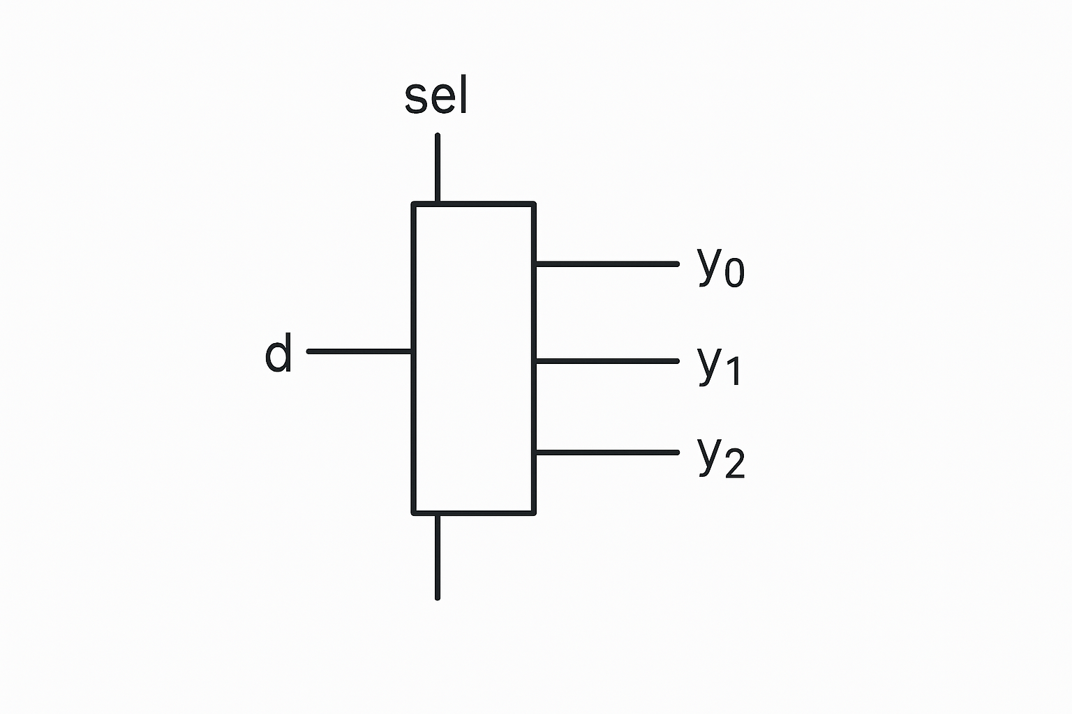
A simple 1‑to‑4 demultiplexer may be written as:
module demux1to4 (
    input  wire       d,
    input  wire [1:0] sel,
    output reg  [3:0] y
);
    always @* begin
        y = 4'b0000;
        y[sel] = d;
    end
endmodule
Such a circuit is useful when a single control signal must be directed to one of many destinations, for example when enabling a particular register or peripheral.
Decoder
Closely related is the decoder. A binary decoder transforms an n‑bit binary input into a one‑hot output vector of size 2ⁿ, in which exactly one line is asserted. For a 2‑to‑4 decoder this looks like:
a1 | a0 | y3 | y2 | y1 | y0 |
|---|---|---|---|---|---|
| 0 | 0 | 0 | 0 | 0 | 1 |
| 0 | 1 | 0 | 0 | 1 | 0 |
| 1 | 0 | 0 | 1 | 0 | 0 |
| 1 | 1 | 1 | 0 | 0 | 0 |
You can read each row as “binary input a1 a0 selects exactly one output bit y0..y3 to be 1.”
A 2‑to‑4 decoder with an enable signal can be specified as:
module dec2to4 (
    input  wire [1:0] a,
    input  wire       en,
    output reg  [3:0] y
);
    always @* begin
        if (!en) y = 4'b0000;
        else case (a)
            2'b00: y = 4'b0001;
            2'b01: y = 4'b0010;
            2'b10: y = 4'b0100;
            2'b11: y = 4'b1000;
        endcase
    end
endmodule
Decoders underpin address decoding in memories, selection of registers, and generation of mutually exclusive control signals.
Encoder
The encoder is the logical inverse: given a one‑hot input vector, it produces the corresponding binary code:
y3 | y2 | y1 | y0 | a1 | a0 |
|---|---|---|---|---|---|
| 0 | 0 | 0 | 1 | 0 | 0 |
| 0 | 0 | 1 | 0 | 0 | 1 |
| 0 | 1 | 0 | 0 | 1 | 0 |
| 1 | 0 | 0 | 0 | 1 | 1 |
Here each row says “if exactly one y line is high, the outputs a1 a0 report its index in binary.”
Assuming exactly one input is high, a 4‑to‑2 encoder may be written as:
module enc4to2 (
    input  wire [3:0] y,
    output reg  [1:0] a
);
    always @* case (y)
        4'b0001: a = 2'b00;
        4'b0010: a = 2'b01;
        4'b0100: a = 2'b10;
        4'b1000: a = 2'b11;
        default: a = 2'b00; // undefined combination
    endcase
endmodule
Priority encoder
In practical systems, however, multiple input lines may be asserted simultaneously. To manage such cases, we employ the priority encoder. A priority encoder resolves multiple active inputs by assigning a fixed ordering: among all asserted inputs, the one with the highest priority determines the output code. It often also produces a validity flag. Conceptually:
 req[7]  ┐
 req[6]  ├─▶ highest index with 1 wins
  ...    │
 req[0]  ┘
An 8‑to‑3 priority encoder in which input 7 has the highest priority can be described as:
module pri_enc8 (
    input  wire [7:0] req,
    output reg  [2:0] idx,
    output reg        valid
);
    always @* begin
        valid = |req;
        casex (req)
            8'b1xxxxxxx: idx = 3'd7;
            8'b01xxxxxx: idx = 3'd6;
            8'b001xxxxx: idx = 3'd5;
            8'b0001xxxx: idx = 3'd4;
            8'b00001xxx: idx = 3'd3;
            8'b000001xx: idx = 3'd2;
            8'b0000001x: idx = 3'd1;
            8'b00000001: idx = 3'd0;
            default:     idx = 3'd0;
        endcase
    end
endmodule
Priority encoders are fundamental in interrupt controllers, resource arbiters, and any context in which multiple requests must be resolved deterministically.
Comparator
Finally, we consider the comparator. A comparator takes two binary numbers and determines their relationship: equality, less‑than, or greater‑than. While it can be implemented hierarchically at the gate level, in Verilog we conveniently express its behavior directly:
module cmp4 (
    input  wire [3:0] a,
    input  wire [3:0] b,
    output wire       eq,
    output wire       lt,
    output wire       gt
);
    assign eq = (a == b);
    assign lt = (a <  b);
    assign gt = (a >  b);
endmodule
Comparators are indispensable in control logic, where branch conditions and decisions depend on the relative values of operands.
In summary, this session has drawn together four strands. Boolean algebra provides the formal language of combinational logic. Karnaugh maps offer a tangible method for simplifying that logic into efficient forms. The TTL tradition reminds us that these abstractions are ultimately realized as fixed functions in hardware. Verilog gives us a modern, scalable means of expressing and composing those functions. The canonical modules we have introduced—multiplexers, demultiplexers, decoders, encoders, priority encoders, and comparators—constitute a vocabulary from which we will construct more complex subsystems: arithmetic and logic units, register files, and eventually complete processors.
In the sessions that follow, we will repeatedly return to these building blocks, combining them according to the principles established here to form increasingly sophisticated digital systems.