Session 3 – Sequential Logic
In this session we move from purely combinational logic to circuits that can remember. These are the circuits that make real computers possible: they keep track of program counters, hold register values, and step through protocols one clock tick at a time.
If any of this feels confusing on a first read, that is completely normal. Most people need to see these ideas several times, in different ways, before they really click. You are not behind, and you are not alone.
By the end of this session, you should have an informal grasp of:
- the difference between latches and flip‑flops,
- how registers and counters are built from flip‑flops,
- how finite state machines (FSMs) use state to model behaviour,
- what setup and hold times mean, and
- why metastability happens and how we mitigate it.
It is okay if you cannot yet work every detail; focus on the big ideas first.
1. From combinational to sequential
Combinational circuits, such as adders and multiplexers, have outputs that depend only on the current inputs. If you give them the same inputs again later, they give the same outputs; there is no memory of the past.
Real systems need to remember things:
- which instruction we are on,
- what data we just loaded,
- what stage of a protocol we are in.
Circuits that remember are called sequential logic.
- They have inputs, outputs, and internal state.
- The state is stored in small memory elements (latches and flip‑flops).
- The state is usually updated on edges of a common clock signal.
The clock gives the whole system a rhythm: “on each tick, everyone updates their state.” That shared rhythm is what makes large designs manageable.
2. Latches – level‑sensitive storage
A latch is a simple storage element that can hold one bit, 0 or 1. A common example is the D latch (“D” for data).
The D latch has three important signals:
D– the data input,Q– the output, andenable– a control signal.

Its behaviour is:
- When
enable = 1(high), the latch is transparent:QfollowsD. IfDchanges,Qchanges as well.
- When
enable = 0(low), the latch holds its value:Qstays at its last value, even ifDchanges.
Key idea: latches are level‑sensitive. They respond whenever the enable signal is at a certain level, not just at a single instant. While the latch is “open” (enable = 1), changes at the input can pass through.
Why this can be tricky:
- In a large design, if several latches are open at the same time, signals can flow through multiple stages in ways that are hard to predict.
- This can create subtle timing problems, especially at high speeds.
Because of this, many synchronous designs prefer to avoid general latch usage and instead use flip‑flops, which are easier to reason about.
If you only remember that a latch is “a 1‑bit memory that is transparent when enabled,” that is enough for now.
2.1 Other latch types (SR and gated SR)
Although we focus on the D latch in this course, it is useful to know the classic SR latch family, because older textbooks and some interview questions still mention them.
SR latch (asynchronous)
- Inputs:
S(set) andR(reset). - Implementation: two cross‑coupled NOR or NAND gates.
- Behaviour (NOR‑based version):
| S | R | Q (current) | Q⁺ (next) | Description |
|---|---|---|---|---|
| 0 | 0 | 0 | 0 | hold (no change) |
| 0 | 0 | 1 | 1 | hold (no change) |
| 1 | 0 | 0 | 1 | set to 1 |
| 1 | 0 | 1 | 1 | stay at 1 |
| 0 | 1 | 0 | 0 | stay at 0 |
| 0 | 1 | 1 | 0 | reset to 0 |
| 1 | 1 | any | invalid | forbidden combination |
- “Asynchronous” here means it reacts immediately to
S/R, without a clock. - The
S=R=1case leads to an unstable or ambiguous state, so most designs avoid it.
Because of this forbidden input combination and the lack of clocking, raw SR latches are rarely used directly in modern synchronous designs.
Gated SR latch
To make the SR latch more controllable, we can give it an enable input:
- When
enable=0, the latch ignoresSandRand simply holds its current value. - When
enable=1, it behaves like the basic SR latch.
Conceptually:
      S --\
           AND ---\
enable ----/       \
                    SR latch → Q
enable ----\       /
           AND ---/
      R --/
This is historically important but still cumbersome because you must manage both S and R and avoid the illegal S=R=1 case. The D latch solves that by collapsing everything into a single data input D, internally generating safe S/R signals.
Verilog template: D latch (level‑sensitive, active‑high enable)
module d_latch (
    input  wire d,    // data input
    input  wire en,   // level-sensitive enable
    output reg  q     // stored output
);
    // When en = 1, q follows d; when en = 0, q holds.
    always @* begin
        if (en)
            q = d;   // no 'else' branch → synthesizer infers a latch
    end
endmodule
Latch types at a glance
| Latch type | Inputs / control | When Q can change | Typical use | Cautions |
|---|---|---|---|---|
| SR latch | S, R | Whenever S=1 (set) or R=1 reset | Rarely used directly; building block for other latches | Illegal S=R=1 in some implementations; fully asynchronous |
| Gated SR latch | S, R, enable | Only while enable=1 | Historical; concept teaching | Still two control signals to manage |
| D latch (level‑high) | D, enable | While enable=1 | Time‑borrowing pipelines, some ASIC flows | Transparency window can cause timing issues if misused |
| D latch (level‑low) | D, enable | While enable=0 | Paired with level‑high latches in 2‑phase clocking | Same transparency concerns, inverted polarity |
In most FPGA‑ and HDL‑based designs you will primarily see D latches, and often you try to avoid inferring them unless you are intentionally using a latch‑based scheme.
3. Flip‑flops – edge‑triggered storage
A flip‑flop is also a 1‑bit storage element, but with more controlled timing. The most common type is the D flip‑flop.
A D flip‑flop has:
D– data input,Q– output, andclk– a clock input.

Its behaviour is:
- On a chosen clock edge (for example, the rising edge when the clock goes from 0 to 1), the flip‑flop samples the value on
Dand copies it toQ. - Between clock edges,
Qstays constant, even ifDchanges.
Key idea: flip‑flops are edge‑triggered.
- They take a “snapshot” of the input exactly at the instant of the clock edge.
- This makes it much easier to predict when things change.
Designers like flip‑flops because:
- all state changes are tied to clock edges,
- you can analyse how long signals have to travel between flip‑flops,
- you can scale up to large, regular synchronous systems.
For now, keep this mental picture:
- Latch – responds over a whole time window when enabled.
- Flip‑flop – responds only at a clock edge.
Verilog template: D flip‑flop (edge‑triggered)
module dff (
    input  wire clk,      // clock
    input  wire reset_n,  // active-low asynchronous reset
    input  wire d,        // data input
    output reg  q         // stored output
);
    // Sample d on the rising edge; reset drives q to 0 immediately.
    always @(posedge clk or negedge reset_n) begin
        if (!reset_n)
            q <= 1'b0;
        else
            q <= d;
    end
endmodule
3.1 Types of flip‑flops and where they appear
In practice you will encounter several named flip‑flop types. Most real hardware primitives can implement them all, but it is useful to know the behavioural differences:
| Flip‑flop type | Inputs | Next state Q⁺ (conceptual) | Typical use | Notes |
|---|---|---|---|---|
| D | D | Q⁺ = D | General storage, registers, pipelines | Dominant in HDL‑based design |
| T (toggle) | T | If T=1, Q⁺ = ¬Q; else Q⁺ = Q | Simple binary counters, divide‑by‑2 | Often implemented as D FF with D = Q ^ T |
| JK | J, K | Q⁺ = J·¬Q + ¬K·Q | Legacy TTL designs, textbooks | Generalises SR; rarely instantiated in RTL |
| SR (clocked) | S, R | Q⁺ = 1 if S=1; Q⁺ = 0 if R=1 | Simple set/reset behaviour | Must avoid S=R=1 depending on design |
Modern RTL almost always uses D flip‑flops, and synthesizers map other descriptions into D‑FF‑based structures.
3.2 Edge polarity and clock enable
- Many libraries provide both positive‑edge and negative‑edge triggered flip‑flops.
- Positive‑edge:
always @(posedge clk) ... - Negative‑edge:
always @(negedge clk) ...
- Positive‑edge:
- You typically choose one edge per clock domain for all your sequential logic to keep timing analysis simple.
Designs often need a clock enable so that a flip‑flop only updates on some cycles. In RTL you should implement this as logic on D, not by gating the clock yourself:
always @(posedge clk) begin
    if (reset)
        q <= 1'b0;
    else if (en)
        q <= d;      // clock enable
    // else: q keeps its old value
end
Under the hood, synthesis tools implement the enable as a multiplexer:
q_next = en ? d : q_current
feeding the D input of a flip‑flop clocked by the ungated clk. This avoids skew and glitch problems that can arise if you try to build your own clock tree with logic gates.
3.2.1 Other named flip‑flops in more detail
T (toggle) flip‑flop (concept and Verilog)
- Behaviour: toggle on each active clock edge when
T=1, hold value whenT=0. - Common use: divide‑by‑2 and ripple counters; conceptual building block.
You can implement a T FF using a D FF with D = Q ^ T:
module tff (
    input  wire clk,
    input  wire reset,
    input  wire t,
    output reg  q
);
    always @(posedge clk) begin
        if (reset)
            q <= 1'b0;
        else if (t)
            q <= ~q;     // toggle when T=1
        // else: hold value
    end
endmodule
JK flip‑flop (concept and Verilog)
- Generalises the SR flip‑flop:
Jacts like “set,”Kacts like “reset,”J=K=1causes a toggle instead of being forbidden.
- Historically important in the 74xx TTL logic family.
One way to implement a JK flip‑flop with a D FF is:
D = J·¬Q + ¬K·Q
In Verilog:
module jkff (
    input  wire clk,
    input  wire reset,
    input  wire j,
    input  wire k,
    output reg  q
);
    always @(posedge clk) begin
        if (reset)
            q <= 1'b0;
        else case ({j, k})
            2'b00: q <= q;      // hold
            2'b01: q <= 1'b0;   // reset
            2'b10: q <= 1'b1;   // set
            2'b11: q <= ~q;     // toggle
        endcase
    end
endmodule
Although JK flip‑flops are a standard topic in textbooks, modern RTL almost always uses D flip‑flops and expresses the desired behaviour directly; synthesis tools map that behaviour onto whatever flip‑flop primitives exist in silicon.
Clocked SR flip‑flop (concept and Verilog)
A clocked SR flip‑flop is simply an SR latch whose input is sampled on a clock edge instead of continuously:
S=1at the edge → set to 1,R=1at the edge → reset to 0,- both 0 → hold,
- both 1 → undefined/forbidden (in the simplest versions).
In Verilog:
module srff (
    input  wire clk,
    input  wire reset, // dominates S/R here
    input  wire s,
    input  wire r,
    output reg  q
);
    always @(posedge clk) begin
        if (reset)
            q <= 1'b0;
        else case ({s, r})
            2'b00: q <= q;      // hold
            2'b01: q <= 1'b0;   // reset
            2'b10: q <= 1'b1;   // set
            2'b11: q <= 1'bx;   // forbidden / avoid
        endcase
    end
endmodule
Because of the awkward S=R=1 case, most real designs prefer D or JK styles when they need set/reset type behaviour.
3.3 Truth tables and state diagrams for basic flip‑flops
You can think of each flip‑flop as a 1‑bit state machine with two states: Q = 0 and Q = 1. The tables below show how the next state Q⁺ depends on the current input(s) and the current state.
D flip‑flop
Truth table (rising edge of clock):
| D | Q (current) | Q⁺ (next) |
|---|---|---|
| 0 | 0 | 0 |
| 0 | 1 | 0 |
| 1 | 0 | 1 |
| 1 | 1 | 1 |
You can see that Q⁺ does not actually depend on the old state: Q⁺ = D.
State diagram:
      D=1             D=1
   ┌───────┐       ┌───────┐
   │ Q=0   │──────▶│ Q=1   │
   └───────┘       └───────┘
      ▲               │
      │               ▼
      └───────────────┘
          D=0 from both states
- If
D = 0at the clock edge, the next state is 0 (from either state). - If
D = 1at the clock edge, the next state is 1 (from either state).
T (toggle) flip‑flop
Truth table:
| T | Q (current) | Q⁺ (next) | Behaviour |
|---|---|---|---|
| 0 | 0 | 0 | hold |
| 0 | 1 | 1 | hold |
| 1 | 0 | 1 | toggle 0→1 |
| 1 | 1 | 0 | toggle 1→0 |
State diagram:
      T=1             T=1
   ┌───────┐       ┌───────┐
   │ Q=0   │──────▶│ Q=1   │
   └───────┘       └───────┘
      ▲               │
      │               ▼
      └───────────────┘
          T=1 toggles

Self-loop on each state when T=0 (hold):
   Q=0 ──(T=0)──► Q=0
   Q=1 ──(T=0)──► Q=1
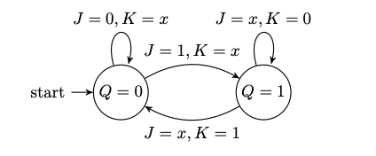
JK flip‑flop
Truth table:
| J | K | Q (current) | Q⁺ (next) | Behaviour |
|---|---|---|---|---|
| 0 | 0 | 0 | 0 | hold |
| 0 | 0 | 1 | 1 | hold |
| 0 | 1 | 0 | 0 | reset to 0 |
| 0 | 1 | 1 | 0 | reset to 0 |
| 1 | 0 | 0 | 1 | set to 1 |
| 1 | 0 | 1 | 1 | set to 1 |
| 1 | 1 | 0 | 1 | toggle 0→1 |
| 1 | 1 | 1 | 0 | toggle 1→0 |
State diagram (grouping input combinations by behaviour):
From Q=0:
  - J=0,K=0 → stay in 0 (hold)
  - J=0,K=1 → stay in 0 (reset)
  - J=1,K=0 → go to 1 (set)
  - J=1,K=1 → go to 1 (toggle)

From Q=1:
  - J=0,K=0 → stay in 1 (hold)
  - J=0,K=1 → go to 0 (reset)
  - J=1,K=0 → stay in 1 (set)
  - J=1,K=1 → go to 0 (toggle)
Graphically:
   Q=0 ──(J=1,K=0 or 1)──► Q=1
   Q=1 ──(J=0,K=1 or 1)──► Q=0

   Self-loops:
   - Q=0 with J=0,K=0 or J=0,K=1 (already 0)
   - Q=1 with J=0,K=0 or J=1,K=0 (already 1)
The compact next‑state equation for a JK flip‑flop is:
Q⁺ = J·¬Q + ¬K·Q
LaTeX/TikZ state diagram for JK flip‑flop
If you would like a drawn state diagram for the JK flip‑flop similar to the FSM diagrams, you can use the following TikZ snippet. Here we compress the input combinations using x to mean “don’t care” (either 0 or 1), and we show that from each state there is:
- a self‑loop when the inputs would keep the state the same, and
- a transition to the other state when the inputs would toggle it.
Clocked SR flip‑flop
Here S means “set” and R means “reset.” The version below assumes the S=R=1 case is treated as “invalid” or “don’t use.”
Truth table:
| S | R | Q (current) | Q⁺ (next) | Behaviour |
|---|---|---|---|---|
| 0 | 0 | 0 | 0 | hold |
| 0 | 0 | 1 | 1 | hold |
| 0 | 1 | 0 | 0 | reset to 0 |
| 0 | 1 | 1 | 0 | reset to 0 |
| 1 | 0 | 0 | 1 | set to 1 |
| 1 | 0 | 1 | 1 | set to 1 |
| 1 | 1 | 0 | ? (invalid) | forbidden |
| 1 | 1 | 1 | ? (invalid) | forbidden |
State diagram (valid cases only):
From Q=0:
  - S=0,R=0 or S=0,R=1 → stay in 0 (hold/reset)
  - S=1,R=0           → go to 1 (set)

From Q=1:
  - S=0,R=0 or S=1,R=0 → stay in 1 (hold/set)
  - S=0,R=1           → go to 0 (reset)
Because the S=R=1 case is problematic in simple SR latches and flip‑flops, most modern designs prefer D, T, or JK flip‑flops, or they wrap SR behaviour in safer higher‑level logic.
4. Registers – storing multi‑bit values
A register is just a group of flip‑flops used together to store a multi‑bit value. For example:
- a 1‑bit flip‑flop stores 1 bit,
- a 32‑bit register uses 32 flip‑flops side by side, sharing the same clock (and usually the same control signals).
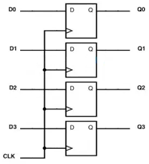
Typical behaviour of a simple register:
- On each clock edge:
- if
load = 1, the register copies its input value to its outputs, - if
load = 0, it keeps its previous value.
- if
You can think of registers as:
- named storage locations inside a CPU (like
x0,x1, …), - pipeline stages between functional units,
- temporary storage inside many digital blocks.
Whenever you see a wide bus labelled “register,” remember that it is really a collection of flip‑flops working together.
Verilog template: parameterised register with load
module reg_n #(
    parameter WIDTH = 8
) (
    input  wire             clk,
    input  wire             reset, // synchronous reset
    input  wire             load,  // load enable
    input  wire [WIDTH-1:0] d,     // data in
    output reg  [WIDTH-1:0] q      // data out
);
    always @(posedge clk) begin
        if (reset)
            q <= {WIDTH{1'b0}};
        else if (load)
            q <= d;
        // else: hold previous q
    end
endmodule
Register types at a glance
| Register type | Key behaviour | Under the hood | Example use |
|---|---|---|---|
| Simple data register | Loads new value when load=1, otherwise holds | Bank of D flip‑flops with enable mux | CPU general‑purpose registers |
| Status/control register | Holds flag bits, often memory‑mapped | Same as data register | Interrupt enables, mode bits |
| Shift register | Shifts left/right each clock, optional serial in | Chain of DFFs; each Q feeds next D | Serial‑to‑parallel, UARTs, serializers |
| Parallel‑load shift reg | Can either load all bits or shift | Data register plus shift‑control muxes | Programmable serial interfaces |
| Pipeline register | Captures intermediate results between blocks | Array of DFFs placed along datapaths | Deep pipelines in CPUs and DSPs |
5. Counters – registers that count
A counter is a register with extra logic that updates it in a pattern, usually by incrementing or decrementing the stored value.
Example: a 4‑bit up‑counter that goes
0000 → 0001 → 0010 → … → 1111 → wraps to 0000
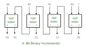
Two common styles:
Ripple (asynchronous) counters
- Each flip‑flop is clocked by the output of the previous flip‑flop.
- Changes “ripple” from the least significant bit to the most significant bit.
- Hardware is simple, but:
- each bit waits for the previous bit to change,
- the total delay grows as you add more bits.
- At high clock speeds this delay becomes a problem.
Synchronous counters
- All flip‑flops share the same clock.
- Combinational logic computes the “next value” (e.g. current value + 1).
- On each clock edge, all bits update together.
- Better suited for fast, synchronous designs.
At an intuitive level, you can think:
- Counter = register + logic that automatically changes its value each clock.
Verilog templates: ripple vs synchronous counters
4‑bit ripple counter (teaching example)
module ripple_counter_4 (
    input  wire clk,    // base clock
    input  wire reset,  // asynchronous reset
    output reg  [3:0] q // count value
);
    // LSB toggles on external clock
    always @(posedge clk or posedge reset) begin
        if (reset)
            q[0] <= 1'b0;
        else
            q[0] <= ~q[0];
    end

    // Each higher bit uses the previous bit as its "clock"
    always @(posedge q[0] or posedge reset) begin
        if (reset)
            q[1] <= 1'b0;
        else
            q[1] <= ~q[1];
    end

    always @(posedge q[1] or posedge reset) begin
        if (reset)
            q[2] <= 1'b0;
        else
            q[2] <= ~q[2];
    end

    always @(posedge q[2] or posedge reset) begin
        if (reset)
            q[3] <= 1'b0;
        else
            q[3] <= ~q[3];
    end
endmodule
In real FPGA designs you usually avoid using data signals as clocks; this module is mainly useful to illustrate ripple timing.
N‑bit synchronous up‑counter (recommended style)
module counter_sync #(
    parameter WIDTH = 4
) (
    input  wire             clk,
    input  wire             reset, // synchronous reset
    input  wire             en,    // count enable
    output reg  [WIDTH-1:0] q
);
    always @(posedge clk) begin
        if (reset)
            q <= {WIDTH{1'b0}};
        else if (en)
            q <= q + 1'b1;
    end
endmodule
Counter types at a glance
| Counter type | Count sequence / direction | Implementation highlight | Pros | Cautions |
|---|---|---|---|---|
| Ripple binary | 0,1,2,3,… in binary | Each bit toggles on previous bit’s output | Very simple hardware | Poor worst‑case timing; not ideal on FPGAs |
| Synchronous binary | 0,1,2,3,… in binary | All bits share clock; next value = q + 1 | Good timing, easy to scale | Slightly more logic than ripple |
| Up/down counter | Up or down, selectable | Next value = q ± 1 based on direction | Useful in stack pointers, timers | Needs careful wrap‑around handling |
| Mod‑N counter | 0…N‑1, then wrap to 0 | Synchronous binary counter plus compare/load | Generates precise periodic events | Must ensure decode logic meets timing |
| Ring counter | One “1” circulates around N‑bit ring | Shift register with feedback | One‑hot state, simple decoding | Uses N flip‑flops for N states (area hungry) |
| Johnson (twisted) | Pattern of ones and zeros circulates | Shift register with inverted feedback | 2N distinct states with N bits | Non‑binary encoding; requires custom decoding |
6. Finite state machines (FSMs)
Many useful circuits cannot be described just as “add one every tick.” They need a notion of state:
- idle vs busy,
- waiting for input,
- sending output,
- error condition, and so on.
A finite state machine (FSM) is a model for such behaviour. It has:
- a finite set of states (S0, S1, S2, …),
- inputs,
- outputs, and
- rules for moving from one state to another.
Hardware view:
- A state register (flip‑flops) holds the current state.
- Next‑state logic (combinational) computes the next state from the current state and inputs.
- Output logic (combinational) computes outputs from the current state (and possibly inputs).
We can draw this as:
Current State (register) ──▶ Next‑State Logic ──▶ Next State (back into register)
                      └────▶ Output Logic ─────▶ Outputs
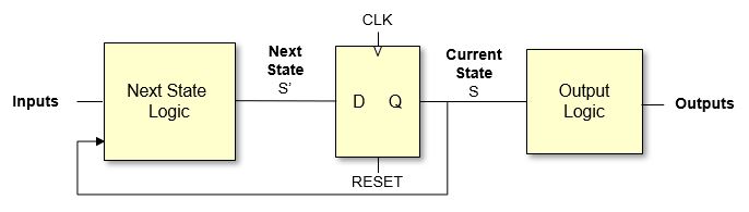
There are two common styles you should recognise.
Moore machines
- Outputs depend only on the current state.
- Outputs change only when the state changes, which usually happens on clock edges.
- This makes outputs less glitchy and easier to reason about.
- Sometimes you need more states to describe the same behaviour.
Mealy machines
- Outputs depend on current state and current inputs.
- Outputs can change as soon as the inputs change, even between clock edges.
- Often uses fewer states and can respond more quickly to inputs.
- Because outputs react directly to inputs, there is more risk of glitches.
You do not have to be able to design big FSMs immediately. For now, remember:
- FSM = state register + next‑state logic + output logic.
- Moore: outputs from state only.
- Mealy: outputs from state and inputs.
Moore vs Mealy at a glance
| Feature | Moore FSM | Mealy FSM |
|---|---|---|
| Output depends on | Current state only | Current state and current inputs |
| When outputs can change | On clock edges (when state register updates) | Any time inputs or state bits change |
| Response speed | At least 1 clock cycle after input change | Can react in the same cycle as input change |
| Glitch risk | Lower – outputs are registered | Higher – purely combinational outputs |
| Output timing analysis | State‑to‑output paths only | State‑to‑output and input‑to‑output paths |
| Typical use | Clean control signals, off‑chip outputs | Fast internal control, sequence detectors |
In practice, you often get the best of both worlds by designing a Mealy‑style FSM for compactness, then registering its outputs so that anything outside the FSM sees clean, clock‑aligned signals.
Verilog templates: small Moore and Mealy FSMs
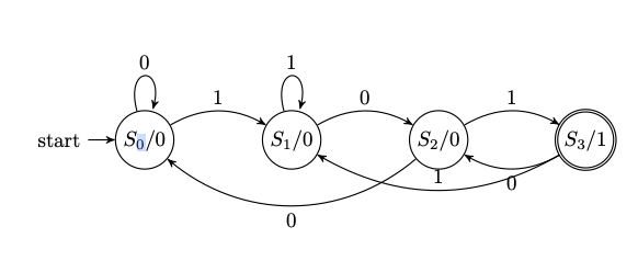
Below is a simple sequence detector that asserts its output when it has just seen the bit pattern 101 on a serial input stream. First in Moore style, then in Mealy style.
Moore FSM: output depends only on state
module seq101_moore (
    input  wire clk,
    input  wire reset,
    input  wire in_bit,
    output reg  match      // 1 when we have just seen "101"
);
    // State encoding
    localparam S_IDLE = 2'b00; // no relevant bits yet
    localparam S_1    = 2'b01; // last bit was 1
    localparam S_10   = 2'b10; // last bits were "10"
    localparam S_101  = 2'b11; // just saw "101"

    reg [1:0] state, next_state;

    // State register
    always @(posedge clk or posedge reset) begin
        if (reset)
            state <= S_IDLE;
        else
            state <= next_state;
    end

    // Next-state logic
    always @* begin
        case (state)
            S_IDLE: next_state = in_bit ? S_1   : S_IDLE;
            S_1:    next_state = in_bit ? S_1   : S_10;
            S_10:   next_state = in_bit ? S_101 : S_IDLE;
            S_101:  next_state = in_bit ? S_1   : S_10; // allow overlapping matches
            default:next_state = S_IDLE;
        endcase
    end

    // Moore output: depends only on state
    always @* begin
        match = (state == S_101);
    end
endmodule
Mealy FSM: output depends on state and input
module seq101_mealy (
    input  wire clk,
    input  wire reset,
    input  wire in_bit,
    output reg  match
);
    localparam S_IDLE = 2'b00;
    localparam S_1    = 2'b01;
    localparam S_10   = 2'b10;

    reg [1:0] state, next_state;

    // State register
    always @(posedge clk or posedge reset) begin
        if (reset)
            state <= S_IDLE;
        else
            state <= next_state;
    end

    // Next-state and output logic
    always @* begin
        match      = 1'b0;   // default
        next_state = state;  // default

        case (state)
            S_IDLE: begin
                if (in_bit)
                    next_state = S_1;
                else
                    next_state = S_IDLE;
            end
            S_1: begin
                if (in_bit)
                    next_state = S_1;
                else
                    next_state = S_10;
            end
            S_10: begin
                if (in_bit) begin
                    // We have just seen "101" → pulse match
                    match      = 1'b1;
                    next_state = S_1;   // overlapping detection
                end else begin
                    next_state = S_IDLE;
                end
            end
            default: begin
                next_state = S_IDLE;
            end
        endcase
    end
endmodule
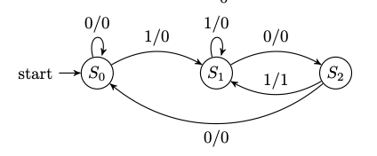
Here:
- In the Moore diagram, each node shows
state / output, and edges are labelled by the input bit. - In the Mealy diagram, each edge is labelled
input/output, and the state circles contain only the state names.
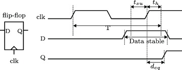
7. Setup time and hold time
In an idealised picture, a flip‑flop would:
- look at
Dexactly at the clock edge, and - instantly and perfectly decide on 0 or 1.
Real hardware is not perfect. The internal circuits need a little time to settle. This introduces two important timing requirements:
- Setup time (
t_setup): how long before the clock edge the inputDmust be stable. - Hold time (
t_hold): how long after the clock edgeDmust remain stable.
A helpful mental picture:
- Take a clock edge (say, rising).
- Around that edge there is a small “forbidden window.”
- The input
Dmust not change during this window. - Instead,
Dshould be stable a bit before (setup) and a bit after (hold) the edge.
If D changes too close to the edge:
- the flip‑flop may capture the wrong value, or
- the flip‑flop may temporarily enter a strange in‑between state (metastability).
In longer paths between flip‑flops:
- the clock period must be long enough for:
- data to leave one flip‑flop,
- pass through the combinational logic,
- arrive at the next flip‑flop,
- and satisfy its setup time before the next clock edge.
You do not need to memorise detailed formulas yet. Just keep the idea that each path has a minimum and maximum safe delay to meet setup and hold times.
8. Timing diagrams – signals over time
A timing diagram is a picture of how signals change over time:
- the horizontal axis is time,
- each signal (clock, inputs, outputs) is drawn as a waveform that goes high and low.
Timing diagrams are useful for seeing:
- when flip‑flops sample their inputs (at clock edges),
- when outputs change after those edges,
- whether setup and hold requirements are respected.
To read a timing diagram:
- Identify the clock waveform and mark the edges that matter (rising or falling, depending on the flip‑flop).
- For each flip‑flop, look at the value of
Djust before the clock edge. - After a small delay, the output
Qtakes this value. - Check whether
Dstayed stable in the setup and hold windows around that edge. - Follow several edges in sequence to see how registers, counters, or FSM states evolve.
At first, timing diagrams can feel busy and intimidating. This is normal. Practice by following one signal at a time and tracing what happens at each clock edge.
9. Metastability – when the flip‑flop is unsure
Metastability is a phenomenon where a flip‑flop, instead of resolving cleanly to 0 or 1, gets stuck temporarily in an in‑between state.
An everyday analogy is balancing a coin on its edge:
- it will not stay perfectly balanced forever,
- eventually it falls to heads or tails,
- but you cannot predict exactly when or which side.
Metastability usually happens when:
- the input
Dchanges during the setup/hold window around the clock edge, - so the flip‑flop’s internal circuits cannot easily decide between 0 and 1.
While metastable:
- the output may be at some undefined voltage between logic 0 and logic 1,
- it may take longer than usual to settle,
- it may cause other logic that reads it to misbehave.
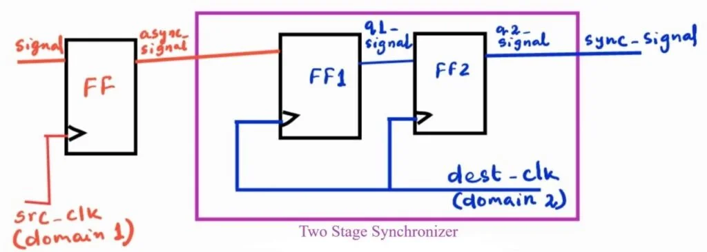
This is especially important when dealing with:
- asynchronous inputs like buttons or external signals not aligned with the clock, and
- clock domain crossings where a signal moves from one clock domain to another.
Physics tells us we cannot completely avoid metastability, but we can make it extremely unlikely to cause a visible error.
Common mitigation techniques:
- For a single‑bit asynchronous signal:
- pass it through a chain of two flip‑flops in the receiving clock domain,
- the first flip‑flop might go metastable, but by the time the second samples it on the next clock edge, it is almost always stable.
- For multi‑bit data:
- use carefully designed schemes such as handshake protocols or asynchronous FIFOs.
Metastability mitigation practices (cheat sheet)
You do not need to be able to derive MTBF formulas to design safe systems. In practice, people follow a small set of standard habits:
| Situation / signal type | What you should do | Why it helps |
|---|---|---|
| Single‑bit async input (button, interrupt line) | Pass through a 2‑ or 3‑flip‑flop synchroniser in the destination clock domain | Gives extra time for any metastability to resolve before the bit is used |
| Multi‑bit async value (e.g. 8‑bit bus) | Do not synchronise each bit separately; use a handshake (valid/ready) or an async FIFO | Ensures all bits are captured from the same “moment in time” |
| Signals between different clock domains | Treat every crossing as a CDC; use synchronisers, handshakes, or dual‑clock FIFOs | Prevents subtle, rare errors that show up only on hardware |
| Asynchronous reset deassertion | Release reset synchronously inside each clock domain (small synchroniser on reset) | Avoids some flops leaving reset slightly earlier than others |
| External noisy inputs (mechanical switches) | Debounce and then synchronise | Debouncing removes rapid toggles; synchroniser handles mis‑alignment with the clock |
| Gated / derived clocks | Prefer a single clean clock plus clock‑enable signals | Reduces unexpected clock edges and skew that can combine badly with metastability |
If you remember nothing else, remember this rule of thumb:
Any signal that is not guaranteed to meet setup/hold timing must be synchronised before you feed it into the rest of your synchronous logic.
Verilog template: 2‑flip‑flop synchroniser
module sync_2ff (
    input  wire clk,       // destination clock domain
    input  wire reset,     // synchronous reset in destination domain
    input  wire async_in,  // asynchronous or other-clock input
    output reg  sync_out   // synchronised output
);
    reg stage1;

    always @(posedge clk) begin
        if (reset) begin
            stage1   <= 1'b0;
            sync_out <= 1'b0;
        end else begin
            stage1   <= async_in; // first stage, may go metastable
            sync_out <= stage1;   // second stage, almost always stable
        end
    end
endmodule
The important message is:
- metastability is real, but
- if you follow standard design practices, systems can run for many years without a metastability‑related failure.
10. If this feels like a lot
It is completely okay if parts of this session felt heavy or blurry. Sequential logic is a big step up from simple combinational circuits. Your brain is building a new mental model, and that takes time.
For now, focus on the big ideas:
- Flip‑flop vs latch – one responds over a window, the other at an edge.
- Register – many flip‑flops storing a multi‑bit value.
- Counter – a register whose value is updated in a regular pattern.
- FSM – a state register plus combinational logic that controls how the state and outputs change.
- Setup/hold – do not change inputs too close to the clock edge.
- Metastability – what happens when that rule is broken, and how we guard against it.
When you work exercises, try to ask:
- Where is the state stored?
- What happens on each clock edge?
- Which signals must be treated as asynchronous and synchronised?
If it does not all make sense yet, that is fine. With repeated exposure, examples, and practice, these concepts become familiar tools. You are doing real computer engineering work here, and feeling stretched is a sign that you are learning something substantial.
11. Technical notes and deeper details
The earlier sections aimed for an intuitive, first‑pass understanding. This section adds more technical detail. Do not feel that you must absorb all of it immediately; it is here as a reference as your comfort grows.
11.1 Latches, time borrowing, and clocking schemes
Internally, a basic latch can be built from cross‑coupled gates:
- an SR latch uses two cross‑coupled NOR or NAND gates,
- a D latch wraps simple logic around an SR latch so that only one data input (
D) needs to be driven.
In modern synchronous design, the most interesting aspect of latches is how they interact with the clock:
- A D latch that is active‑high is transparent when
clk = 1and opaque whenclk = 0. - An active‑low latch is transparent when
clk = 0and opaque whenclk = 1.
If you build a pipeline using two non‑overlapping clock phases (ϕ1 and ϕ2), you can alternate active‑high and active‑low latches so that:
- information flows during
ϕ1through the first set of latches, - then during
ϕ2through the second set, and so on.
Because a latch is transparent for a finite window, it can borrow time from the following stage: if combinational logic on one side of a latch is slow and the logic on the other side is fast, the latch’s transparency window gives the slow side a little extra time beyond a single clock edge. High‑performance ASIC designs sometimes exploit this.
On FPGAs and in introductory courses, however, unrestricted latch use is discouraged because:
- reasoning about time borrowing and transparency is harder than reasoning about edge‑triggered behaviour, and
- many FPGA fabrics provide only flip‑flop primitives, not general latches.
Synthesis tools will infer a latch whenever your RTL describes “remember the old value when this condition is false.” For example in Verilog:
always @* begin
    if (en)
        q = d;  // no else branch → latch inferred
end
In synchronous designs you typically want to avoid such implicit latches unless you are very sure you need them.
11.2 Flip‑flops, master–slave structure, and timing parameters
An edge‑triggered D flip‑flop is often implemented internally as two latches in series:
- a master latch that is transparent when
clk = 1, - a slave latch that is transparent when
clk = 0.
On the rising edge:
- the master latch stops tracking
Dand holds its last value, - the slave latch becomes transparent and updates its output from the master.
By careful design of the clocking and device physics, the combined behaviour approximates a single instant of sampling at the edge.
Device data sheets specify several important timing parameters for flip‑flops:
t_clk→Q(ort_cq): clock‑to‑Q delay – how long after the active clock edge the outputQis guaranteed to be valid.t_setup: setup time – how long before the clock edgeDmust be stable.t_hold: hold time – how long after the clock edgeDmust remain stable.t_pw: minimum clock pulse width – how long the clock must stay high and low.
Note that t_clk→Q, t_setup, and t_hold often come in minimum and maximum values, reflecting process, voltage, and temperature variations.
Flip‑flops also often include:
- asynchronous reset or preset inputs (force
Qto 0 or 1 immediately), and/or - synchronous reset inputs (applied only on the next active clock edge).
Asynchronous resets are convenient for bringing a system into a known state at power‑up, but they themselves can cause metastability if not carefully released relative to the clock. Synchronous resets avoid that issue at the cost of slightly more logic.
11.3 Registers, enables, and bus structures
Registers rarely exist in isolation; they form part of larger bus structures:
- A register file in a CPU might contain 32 registers of 32 bits each, with two read ports and one write port.
- Each register typically has:
- a clock (
clk), - a write enable (
we), - data input (
d[n:0]), - output (
q[n:0]), - and possibly a reset.
- a clock (
In synchronous RTL, a typical register with enable is written:
always @(posedge clk) begin
    if (reset)
        q <= 0;
    else if (we)
        q <= d;
end
- The non‑blocking assignment (
<=) reflects that all flip‑flops update conceptually in parallel on the clock edge. - The
if (we)implements the load/hold choice without generating unintended latches because this always block is edge‑triggered, not level‑sensitive.
Multi‑port register files (e.g. with two independent read addresses) are typically implemented using either:
- replicated storage arrays with separate read ports, or
- specialised hard blocks in FPGAs or memory compilers in ASIC flows.
11.4 Counter design and variants
You can view counters as a special case of FSMs with a regular state pattern. A few further details:
- In ripple counters, each flip‑flop often operates as a T (toggle) flip‑flop:
T = 1makes the bit toggle whenever its “clock” input toggles,- connecting each
Qto the “clock” of the next bit produces a binary count sequence.
- In synchronous counters, next‑state logic is derived from the binary increment function:
- bit 0 toggles every cycle,
- bit 1 toggles when bit 0 is 1 and will wrap to 0,
- bit 2 toggles when bits 1:0 are both 1 and will wrap, and so on.
Practical counters often have:
- a synchronous clear or load input to set an initial value,
- enable signals to gate counting,
- wrap‑around at a configurable modulus
N(mod‑N counters), - decoded outputs such as “terminal count” pulses when the counter reaches a particular value.
For example, a mod‑10 decimal digit counter (0–9) must detect when the internal binary count reaches 9 (1001₂) and then load 0 on the next cycle instead of 10. Such “truncated” counters appear in timers, frequency dividers, and digital clocks.
11.5 FSM realisation and state encoding
Formally, a synchronous FSM is defined by:
- a state set
S, - an input alphabet
I, - an output alphabet
O, - a next‑state function
δ : S × I → S, - and an output function:
- for Moore,
λ : S → O, - for Mealy,
λ : S × I → O.
- for Moore,
In hardware, you must choose a concrete encoding for the abstract states:
- Binary encoding:
- use
⌈log₂ |S|⌉flip‑flops, - states are assigned binary codes (e.g. S0 =
00, S1 =01, S2 =10, S3 =11), - area‑efficient but next‑state logic can be more complex.
- use
- One‑hot encoding:
- use one flip‑flop per state,
- exactly one flip‑flop is 1 at any time,
- simplifies next‑state and output logic (often just simple AND/OR),
- attractive on FPGAs where flip‑flops are plentiful and logic depth matters.
- Gray encoding:
- adjacent states differ in only one bit,
- useful when you want to minimise glitches in decoded logic (and for some FIFO pointer schemes).
There are trade‑offs among area, speed, and ease of debugging. Many synthesis tools can choose an encoding automatically, but it is important to understand the implications.
Moore vs Mealy timing in more detail
There are three main kinds of timing path to think about in an FSM:
- State → next state (through the next‑state logic to the state register inputs),
- State → outputs (through Moore‑style output logic), and
- Inputs → next state / outputs (paths that exist only in Mealy‑style machines).
In a Moore machine:
- Outputs depend only on the state bits.
- The only relevant timing paths for outputs are state FFs → output logic → output pins.
- Outputs therefore change in a controlled way shortly after each active clock edge, and static timing analysis treats them like any other registered signal path.
In a Mealy machine:
- Outputs depend on both state bits and raw inputs.
- There are additional combinational paths:
- inputs → output logic → outputs, and
- inputs → next‑state logic → state FFs.
- Any hazard or short glitch on an input can momentarily ripple through the logic and cause a spurious pulse on a Mealy output, even if the state has not changed.
Common timing mistakes with Mealy outputs:
- Driving off‑chip pins or other clock domains directly from Mealy outputs:
- because the outputs are combinational, they can violate setup/hold timing in the receiving domain or be seen as multiple pulses due to glitches.
- Using a narrow, glitchy Mealy output as an enable for another register:
- a short spike might be interpreted as a clock enable pulse, causing an extra, unintended update.
- Forgetting that Mealy outputs can change between clock edges:
- makes it harder to reason about protocol timing if the consumer expects changes only at edges.
A very common and robust pattern is:
- design the internal logic as a Mealy FSM (small, fast), but
- register all externally visible outputs (
always @(posedge clk) out_reg <= out_mealy;), - and treat
out_regas the “real” output used by the rest of the system.
This effectively turns the machine’s external interface into a Moore‑style view, while keeping the internal implementation compact.
11.6 Formal timing constraints: max frequency and hold safety
Consider a simple synchronous path:
clk → [FF₁] → combinational logic → [FF₂] → …
Let:
t_clk→Q_maxbe the maximum clock‑to‑Q delay ofFF₁,t_comb_maxbe the maximum propagation delay through the combinational logic,t_setupbe the setup time ofFF₂,t_skewbe the worst‑case clock skew betweenFF₁andFF₂.
To guarantee that FF₂ samples the correct value, the clock period T_clk must satisfy:
T_clk ≥ t_clk→Q_max + t_comb_max + t_setup + t_skew
This inequality defines the maximum clock frequency:
f_max ≤ 1 / T_clk_min
where T_clk_min is the smallest clock period compatible with the worst‑case delays.
Hold time imposes a different constraint. Let:
t_clk→Q_minbe the minimum clock‑to‑Q delay ofFF₁,t_comb_minbe the minimum delay through the combinational logic,t_holdbe the hold time ofFF₂.
To avoid a hold violation, we require:
t_clk→Q_min + t_comb_min ≥ t_hold + t_skew
If the left‑hand side is too small, the new data might reach FF₂ so quickly that it overwrites the old data before the hold window has closed.
Design flows therefore:
- check setup constraints on all paths to determine
f_max, and - check hold constraints to ensure there are no excessively fast paths.
Fixes:
- For setup violations: lengthen the clock period, pipeline the logic (insert another register), or optimise/shorten the critical combinational path.
- For hold violations: add intentional delay (buffers) to very fast paths or balance clock skew.
When an FSM is “mistimed,” one of these inequalities has effectively been broken on some path:
- a state‑to‑state path (critical path in the control logic),
- a state‑to‑output path (Moore output arrives too late for whatever uses it),
- or, in Mealy designs, an input‑to‑output path (Mealy output transitions too slowly or glitches right when another block samples it).
Such violations may not show up in simple simulation, which assumes ideal timing, but they will show up as setup/hold failures in static timing analysis or as occasional misbehaviour on real hardware.
11.7 Timing diagrams with propagation and contamination delays
For more precise timing analysis, combinational logic is modelled with two parameters:
- propagation delay (
t_pd): the maximum time from an input change to the corresponding output change, - contamination delay (
t_cd): the minimum time before an output might start to change after an input change.
The earlier setup‑time inequality uses t_pd (worst‑case) to guarantee that data arrives soon enough; the hold‑time inequality uses t_cd (best‑case) to guarantee that data does not arrive too early.
In a detailed timing diagram you may see:
- a clock edge at time
t₀, Qof a launching flip‑flop changing slightly aftert₀(byt_clk→Q),- outputs of intermediate gates changing in a staircase fashion, each delayed by their own
t_pd, Dof the capturing flip‑flop reaching its final value before the next clock edge, with the required setup margin.
Understanding these diagrams is the bridge between the intuitive “snapshot at each clock edge” model and the physical reality of signals propagating with finite speed.
11.8 Metastability metrics and CDC practices
Metastability can be modelled statistically. A common simplified model states that the mean time between observable failures (MTBF) of a synchroniser grows exponentially with the available resolution time T_res:
MTBF ≈ (1 / (f_clk · f_data · C)) · e^(T_res / τ)
where:
f_clkis the receiving clock frequency,f_datais the rate of asynchronous input events,Candτare device‑dependent constants extracted from silicon,T_resis the time between the first flip‑flop’s sampling edge and the second flip‑flop’s sampling edge (roughly one clock period minus some margins).
By adding an extra flip‑flop stage (increasing T_res), you can increase MTBF by several orders of magnitude. Designers target MTBFs far longer than the expected lifetime of the product (years or centuries) so that metastability‑induced failures are practically negligible.
For clock domain crossings (CDC) of multi‑bit values, simple bit‑by‑bit synchronisation is unsafe because different bits may be captured on different cycles. Common techniques include:
- handshake protocols (valid/ready, request/acknowledge):
- data is only considered valid when both sides agree via synchronised control signals;
- dual‑clock FIFOs:
- use separate write and read pointers in their respective clock domains,
- encode pointers in Gray code so only one bit changes at a time,
- synchronise the Gray‑coded pointers across domains and compare them to detect full/empty conditions.
Industrial design flows include dedicated CDC analysis tools that check for unsafe crossings and verify that appropriate synchronisation structures are used.
These details are not required for first‑pass intuition, but they become essential when you push designs to higher performance or integrate multiple clock domains on a single chip.